Pinhole alignment in a confocal microscope
For citeable PDF versions of this document, please use the links below.
- DOI (concept): https://doi.org/10.5281/zenodo.3663866
- DOI (version): https://doi.org/10.5281/zenodo.3894896
- Authors: Azmeen Rahman, Jiahe Cui and Martin Booth
- Last modified: 5 yrs ago
The listed authors have participated in the writing of this document. As the content is the culmination of long term work in the Dynamic Optics and Photonics Group, many others have contributed directly or indirectly to this material. We consciously acknowledge all of these contributions, even though it is impractical to list them all here
Abstract
We present two protocols for the alignment of the pinhole in a confocal microscope. The first utilizes motorized scans in the X-Z plane; while the second addresses the condition with only manual axial translation. Both protocols are relevant for reflection and fluorescence mode confocal microscopes.
Introduction
The two protocols explain how to align the position in three-dimensions of the pinhole in a confocal microscope. The alignments are performed in reflection mode, but the processes are also relevant for fluorescence mode microscopes. Removal of the emission filter from a fluorescence mode microscope is usually sufficient to perform reflection mode imaging, as the dichroic filter typically passes a small proportion of the light reflected from the specimen through to the detector. After alignment, the emission filter can usually be replaced without any significant detrimental effects on the imaging performance.
The first protocol demonstrates the alignment procedure for when the function of performing motorized scans of the X-Z plane is available, e.g. by using an objective piezo scanner or a motorized sample stage. The second protocol explains how the alignment of the pinhole can be achieved without a motorized X-Z scan function. In the latter case, a motorized X-Y scan function, a sample stage with manual axial translation, and an oscilloscope is required.
1. Alignment with motorized X-Z scan
A 633nm laser was used in the demonstration with a 150 mm lens focusing the light reflected from the specimen into a photomultiplier tube. Consequently, the diameter of the first zero of the Airy disk of the focal spot was approximately 93 µm. For good imaging, any pinhole of diameter between 0.25 and 1 of the Airy disk diameter may be used. In this particular microscope, a confocal pinhole of diameter 20 µm was used. Additionally, as part of the alignment process, a larger pinhole of diameter 800 µm was used. Accordingly, any pinhole of diameter between 5 and 10 of the Airy disk diameter may be used for the latter situation.

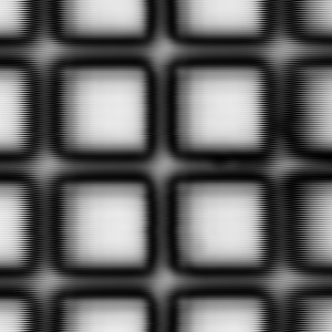
Figure 1 shows an illustration of the test specimen used in the pinhole alignment procedure (e.g. Agar Scientific silicon test specimen AGS1930). The specimen has a reflective surface with raised square blocks of periodicity 10 μm and gap spacing of 1.9 μm. The height of the blocks is around 100 nm. Any other reflective specimen with sub-wavelength height surface structure might also be used. The directions corresponding to the X, Y and Z scans used in the process are also shown in the diagram.
1.1 Imaging without a pinhole
-
Place the test specimen, shown in Figure 1, on the stage.
-
Attach the larger pinhole before the PMT.
-
Image the specimen in the X-Z plane.
-
Use a marker or cursor to mark the position of the specimen surface, which corresponds to dark marks on the image (see Figure 2).
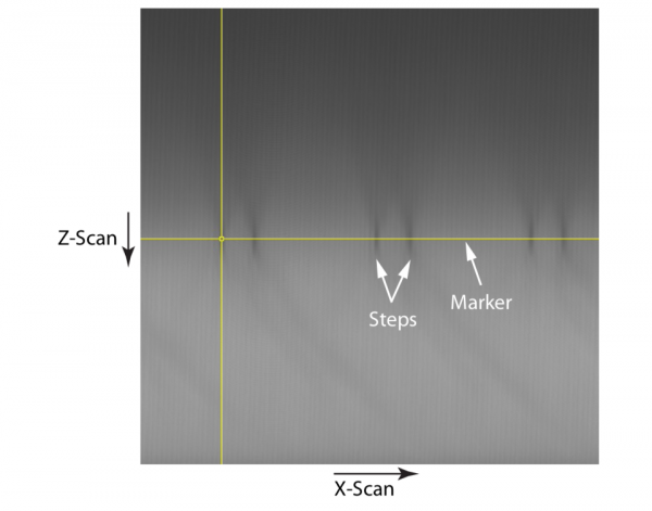
The specimen should be mounted in the appropriate immersion medium (e.g. water for a water immersion lens). It will be scanned in the X-Z plane. Using the larger pinhole provides similar imaging to having no pinhole, but at the same time it protects the PMT from excessive exposure to ambient light and subsequently saturating the detector. All the light reflected by the specimen is collected by the PMT. During the axial scan, light is diffracted away from the pinhole due to the step edges of the square blocks. These steps, therefore, appear as regions of low signal in the image, which can be clearly observed in Figure 2. The marker is used to indicate the position of the steps, and hence the surface of the specimen. This position will be used in the following steps to ensure that the confocal pinhole is in the correct Z plane so as to image the steps and the surface of the specimen.
1.2 Imaging with pinhole
-
Attach the small confocal pinhole before the PMT.
-
Image the specimen in the X-Z plane.
-
Adjust the pinhole in X-Y (so that light passes through it into the PMT) until a strong signal is received from a plane of the specimen (see Figure 3).
-
Translate the lens focussing light onto the confocal pinhole along the axis until the plane imaged coincides with the marker (as set in the previous step using the large pinhole). The steps should now be visible, see Figure 4.
-
Adjust the pinhole in X-Y again until a strong signal is received.
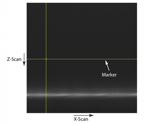
The specimen is scanned in the X-Z plane with a confocal pinhole in place. Figure 3 shows the confocal image when the pinhole is in the incorrect Z-plane and its X-Y position adjusted for optimal signal. The mirror-like specimen is not in the focal plane, but still creates a focus at the confocal pinhole when in a particular defocused plane and so light is detected with the specimen in this Z position (compare the position with that seen in Figure 2). However, as the steps are out of focus, they cannot be seen in the image.
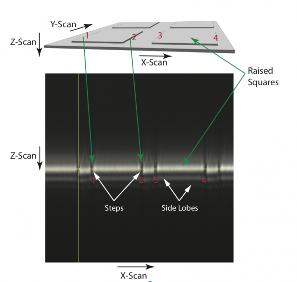
The pinhole must be moved to the correct Z position, such that light from the desired plane (i.e. the surface of the specimen where the steps are visible, see Figure 2) is detected by the PMT. This is accomplished by moving the lens that focuses light on the confocal pinhole along the axis until the plane of light coincides with the marker, as shown in Figure 4. Once in the correct plane, the steps might not be visible at once. The pinhole must be adjusted in the X-Y plane for optimal signal. This process ensures that the confocal pinhole has been aligned in the correct Z plane.
1.3 Correction of aberrations
Residual aberrations may still be present in the system. While a full adaptive optics approach can be used to correct these, some simple steps can be taken using the mirror specimen, especially when using a water immersion lens with a correction collar for compensation of spherical aberration.
-
Image the specimen in the X-Z plane.
-
Adjust the correction collar.
-
Search for a collar setting with maximum peak intensity. This should also correspond to the narrowest axial response.
-
Minor adjustment of the pinhole may lead to increased signal after correction of spherical aberration.
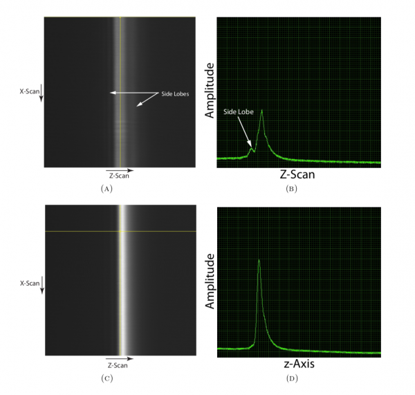
The mirror is scanned in the X-Z plane now that the confocal pinhole is aligned. Figure 5(A) shows the image as the mirror is scanned through the focus; the contrast is poor owing to system aberrations. Figure 5(B) shows the cross-section of the image. Due to the aberrations, the peak is not sharp and side lobes may be observed. Adjustment of the correction collar should alter the amount of spherical aberration that affects the axial response. At the optimal position the peak of the response should be maximized, and the width of the response should be minimized. The response may not be symmetric, as residual aberrations might be present even after correction with the collar, which can only provide approximate compensation. Further correction would require the use of an adaptive optical element, such as a deformable mirror.
2. Alignment without motorized X-Z scan
A 830 nm super-luminescent diode (SLD) was used with an adjustable fibre collimator (Thorlabs CFC-11X-B) that incorporated a 11 mm aspheric focusing lens to focus the reflected light from the same silicon grid sample as in Figure 1 (Agar Scientific silicon test specimen AGS1930) into a 5 μm single mode fibre (Thorlabs P3-830A-FC-2), which is then connected to a silicon avalanche photodiode (APD430A/M). One Airy unit was equivalent to 6.55 μm in the system, and a fibre core size around 0.7 Airy unit was used. Multimode fibres with larger core sizes were also chosen to effectively implement the alignment procedure (50 μm, 25 μm and 10 μm). A manual XYZ differential translation stage (Thorlabs PT3A/M) was used to translate the silicon grid.
The main necessity of this alignment protocol is to deal with complications arising from the fact that the highest detected signal does not necessarily correspond to the correct pinhole position, but rather a particularly defocused one. This can be effectively solved by using an oscilloscope and computer GUI interface to simultaneously monitor signal amplitude and the fidelity of X-Y scan images of the grid surface. The selected FOV should preferably incorporate 2-4 grids so that the images of individual grid structures are large enough for changes to be differentiated by eye on the GUI interface, while also allowing for the monitoring of relative changes between adjacent grids. Sensitivity of the changes can be enhanced by adopting sub-wavelength-height surface structures, as in the reflective specimen used in this protocol.
2.1 Imaging with no pinhole
-
Image the specimen in the X-Z plane. Attach one end of the 50 μm fibre to the detection collimator and the other end to the APD. Attach both the computer with scanning and image acquisition software and the oscilloscope to the detector and leave the software scanning in X-Y mode. Leave the distance between the focusing lens and fibre tip to the minimum in the collimator for now. We are aiming for a grid-shaped image on the software while achieving the highest possible stepping flat-top signal on the oscilloscope.
-
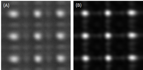
Bring the sample stage away from the objective such that the objective focal plane is between the sample surface and the objective itself. Then gradually translate the sample stage towards the objective using the differential adjusters. There will be alternating cycles on the GUI interface of patterns that resemble the grid surface coming in and out of focus. Typical out-of-focus patterns are illustrated in Figure 6. Within the first few cycles of the alternating patterns, the SNR of the images and the signal level on the oscilloscope will both be low, as depicted in Figure 6(A). Then there will be a point when the signal on the oscilloscope becomes significantly stronger and the image SNR much higher throughout the whole cycle, as depicted in Figure 6(B). This is the cycle of alternating patterns that indicate the grid surface being within vicinity of the nominal focal plane, though the axial position of the fibre pinhole still needs adjustment and will be dealt with later. The shapes of the patterns look similar to those seen in previous cycles. After this cycle, if the sample stage is translated closer to the objective, the signal and SNR will drop significantly and resemble what is seen in Figure 6(B) again.
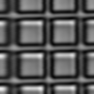
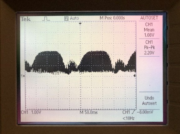
- Within the cycle close to the nominal focal plane determined in Step 2.1.2, fine adjust the sample stage to a position where the image best resembles the shape of in-focus square grids. Figure 7 gives an example of how the image would look at a near optimum axial position using the 50 μm fibre. Note how the dark square rings are even on all sides of the grid. At the same time, monitor the oscilloscope to check that the signal has a stepping flat-top profile, as depicted in Figure 8. This flat-top profile should not be compensated for a higher signal with a triangular profile, which would lead to substantial amounts of defocus.
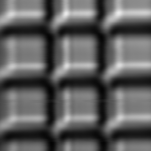
- Note that throughout the process of translating the sample stage axially, the individual square grids should look as centred and symmetrical as possible within its localised position. Any signs of shadows or edges of the grid merging into the background, as shown in Figure 9, would suggest a lateral displacement of the fibre pinhole, and the need for X/Y translation of the fibre mount to bring the grid images towards a more centred position where no shadows of grids are present any more. These effects would be more prominent in later steps using smaller core size fibres as they are more sensitive to lateral displacement.
2.2 Imaging with large pinholes
-
Unscrew the 50 μm fibre and change to the 25 μm fibre. A low SNR grid image should be present straight away. If not, change back to the 50 μm fibre to adjust the axial position of the sample stage and lateral position of the fibre mount until an image is present upon switching to the 25 μm fibre.
-
Fine adjust the sample stage again to obtain the highest possible stepping flat-top signal on the oscilloscope while monitoring the fidelity of the square grid surface on the GUI interface. In the meanwhile, pay attention to Step 2.1.4. Then start to adjust the axial distance between the focusing lens and fibre tip in the fibre collimator. Alternate the process of fine adjusting the axial position of the sample stage, axial translation of the fibre collimator and X/Y translation of the fibre mount so as to achieve the highest stepping flat-top signal possible on the oscilloscope, while monitoring the fidelity of the square grid surface in the GUI interface.
-
When Step 2.2.2 is achieved with the 25 μm fibre, repeat Steps 2.2.1 and 2.2.2 with the 10 μm fibre before switching to the 5 μm fibre.
2.3 Imaging with a small pinhole
- Repeat Steps 2.2.1 and 2.2.2 with the 5 μm fibre. Figure 10 shows one example of the X-Y scan image acquired when the sample plane and 5 μm fibre are both at a near optimum position.
